That is a fine reason for doing the project. Learning hands on beats book learning .
I agree with Neville a great way to learn by doing. It’s been a long time since I taught electronics (35 years) and used breadboards for projects with students to explain principles. We move so quickly.
Sorry for not posting for a long time as I was busy with my studies. But now I have started building the 8bit CPU and I wanted to share some of the Updates here today.
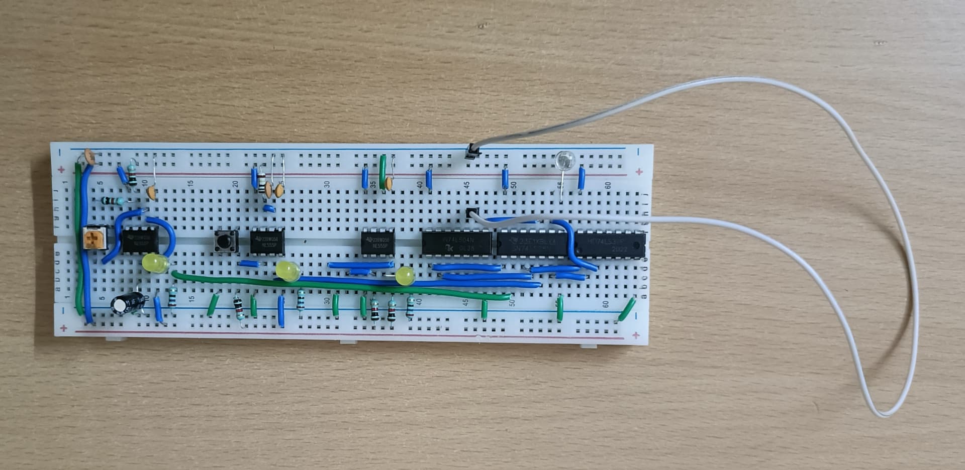
The first photo shows the clock circuit. This circuit is not yet complete due to the absence of some switches. I have placed an order for the switched but they are yet to be delivered. In the clock circuit I used NE555 timer and have created three separate circuit using the NE555 timer one is a astable circuit, monostable circuit and a bistable circuit. The monostable circuit is used to provide an automatic clock response, the monostable circuit is used to provide a way for putting in manual clock pulse especially running a program slowly for the purpose of debugging the problem. And the bistable circuit is used to choose between the astable and monostable forms.
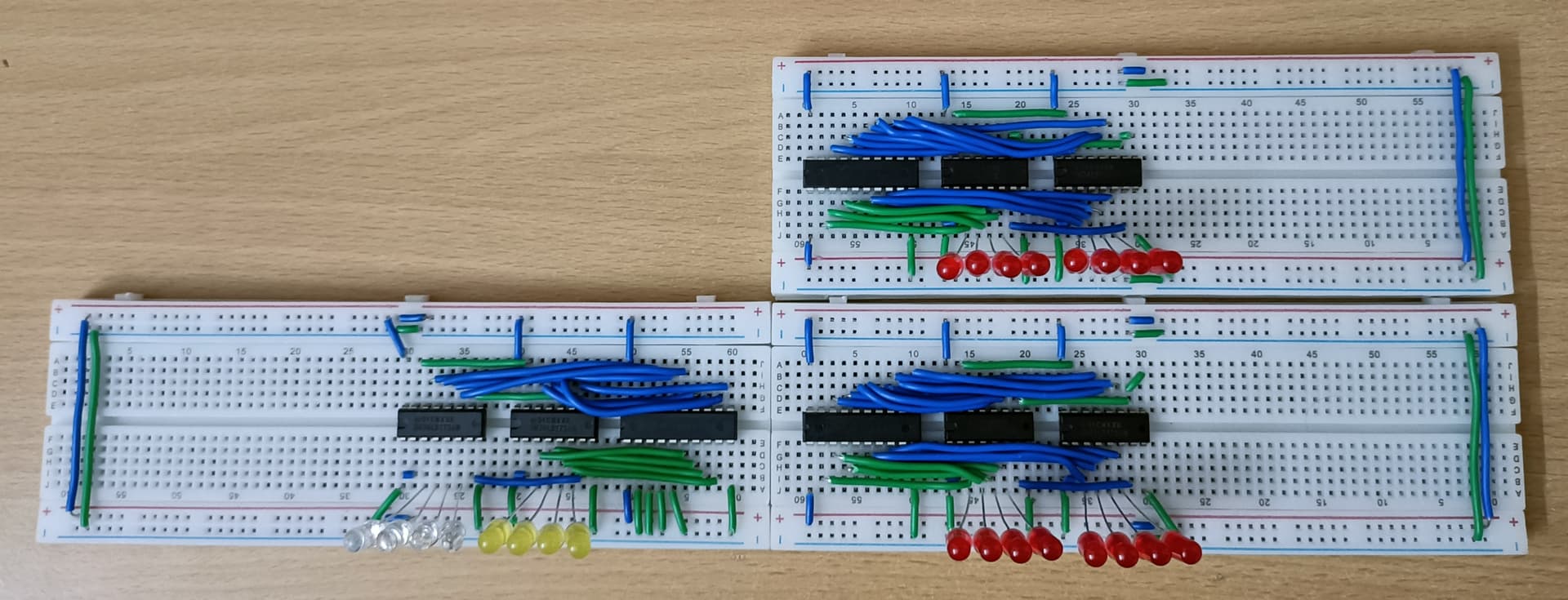
The second pictures are the pictures of the three registers that i have built register A, register B and the Instruction Register. For building the registers I have used the concept of D flip flop along with a tristate logic to prevent the output value from the D flip-flop from changing continuously. I could have built D flip-flop circuit using the AND and OR logic gates but for that I had to build 8 separate D flip-flops for the purpose of storing 8bit data. So this would be cumbersome and would also leave me with a lot of troubleshooting and places for errors and noise to creep into the circuit, which will be undesirable. So i instead for the 74LS173 IC, which is a 4 bit register and a D flip-flop. I have used two 74LS173 IC in the circuit. In the circuit I have also used a 74LS245 Octal Bus transmitter/receiver, to send data to the bus which will be build once all the components are completely built.
If any of you have some questions regarding the technical aspect or have some suggestions to improve my approach or have any thoughts on this project, please don’t hesitate to reply back to this post.
Hi @Arghadeep_Saha ,
i do not personally have
enough electronics to understand your project, but I must say we appreciate
your detailed reply. Keep us informed
Regards
Neville
That’s GREAT!!! ![]()
Reading your post I feel back in my youth in 1991…
![]()
Oh, those good old times…
Thanks for the update and sharing of the photos. Been a very long time since I used a 555 and breadboard for any build projects with my students before getting them to create PCBs.
It’s a great way to learn electronics from a practical stance not just read about it. Could work out expensive in the long run but hope that does not put you off.
Look forward to the next update
Hi @Arghadeep_Saha,
First of all, congrats for your project.
I’ve only just seen your post and I’m going to take the opportunity to add a few more websites to the list:
I know more, but they’re in Europe…
If you need a program to make the schematics or PCBs design, you could try KICAD
To manufacture PCBs, see these websites:
See if these electronics forums interest you:
- EEVblog Electronics Community Forum
- Electrical Engeneering (may not be considered a forum)
- Reddit, in particular, maybe the r/beneater community, which is in line with your project, and Ben Eater on YouTube.
here’s a link to a project on GitHub that might be similar to yours, so you can get some ideas
I’d like to ask you a few questions if you don’t mind:
You mentioned that you follow a guided tutorial. Is it possible for you to post the schematic of your project here and the changes you made?
I can’t see well in the picture: is it the the 74LS173A, correct?
I don’t intend to comment on your schematic, because what you have is very positive and an excellent way to learn, but I’m just going to give you my opinion on a subject that may be controversial:
- You have the LEDs connected directly to the Flip-Flops. Have you already checked the datasheet for the IC’s maximum output current? And the LEDs, how can you limit the current of each LED?
I don’t know the manufacturer of your 74LS173, but here’s the link to the SN74LS173A
As @nevj and @callpaul.eu said, keep us informed
Best of luck for your project
Jorge
Hi @Tech_JA,
First of all sorry for the late reply, I was busy with my university exams and project submission.
You are correct about the fact that I directly connected the LEDs to the 74LS173 chips and you will find that I have connected the LEDs directly to the ICs in every circuits shown above. This decision is technically incorrect and is shown problems in the working of the LEDs, like the LEDs are not glowing that brightly and they are constantly blinking with the clock. But my decision of not including the resistor here is purely to keep the circuit clean. As you can see from the picture the wires occupy the entire breadboard and it would be very difficult to cram the resistors in between. But once I build the entire CPU and then shift it to a printed PCB I will make sure to add those resistors or perhaps exchange these LEDs with ones that have resistors in built.
Thank You for your suggestion
Arghadeep
First of all let me apologise for not posting the updates of my project for this long.
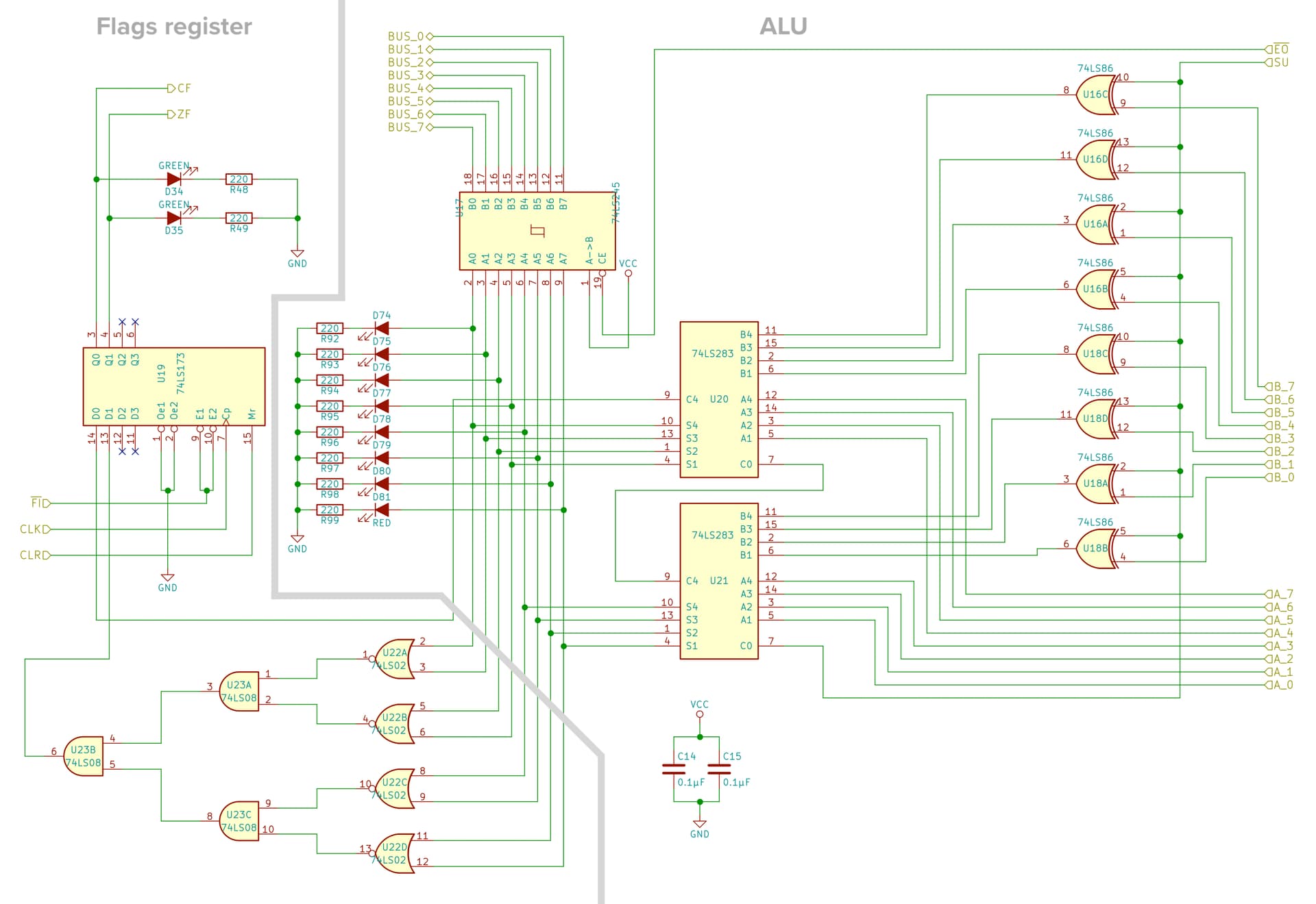
So please allow me to introduce you to the ALU of the 8bit CPU that I am working on taking inspiration from various online articles.
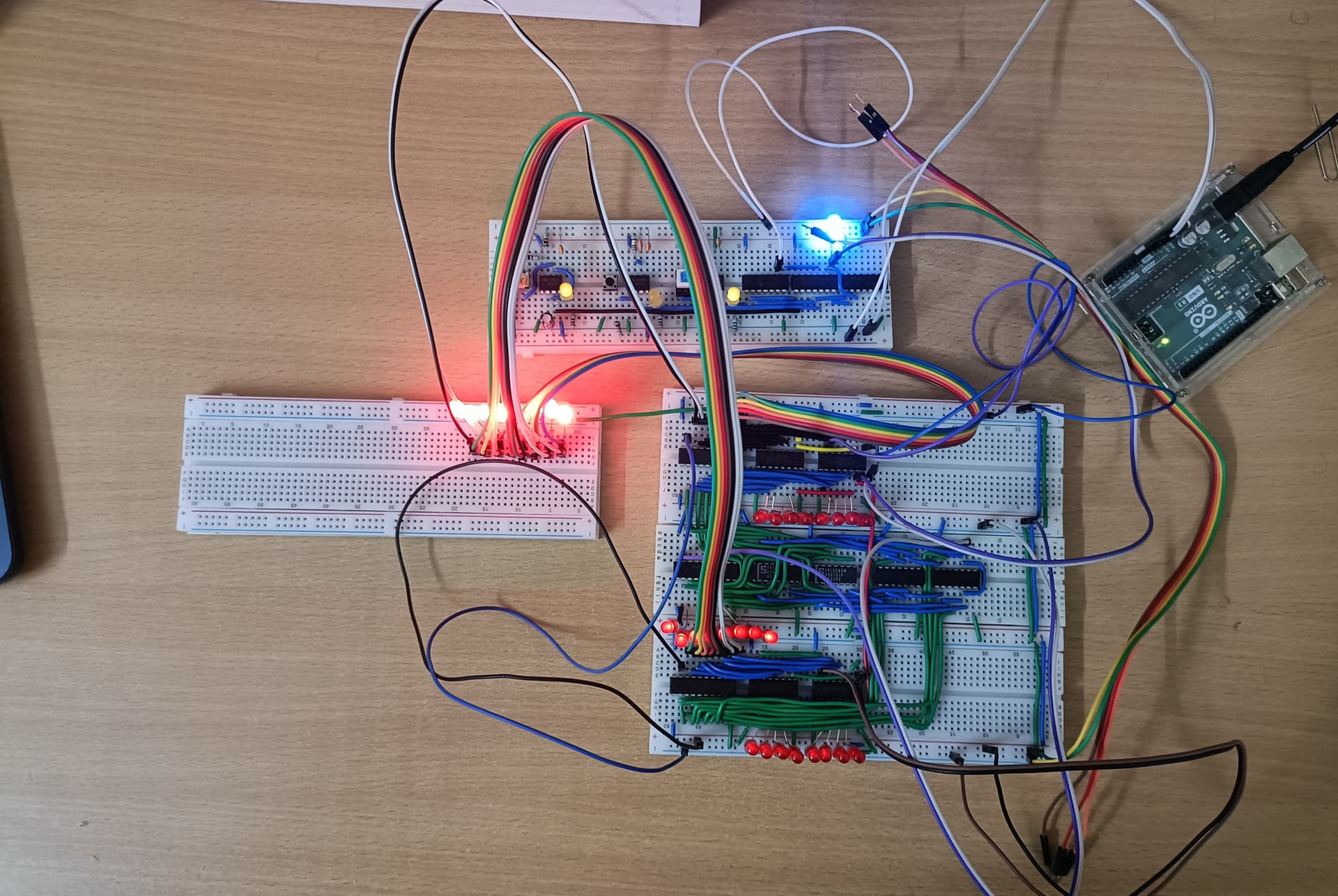
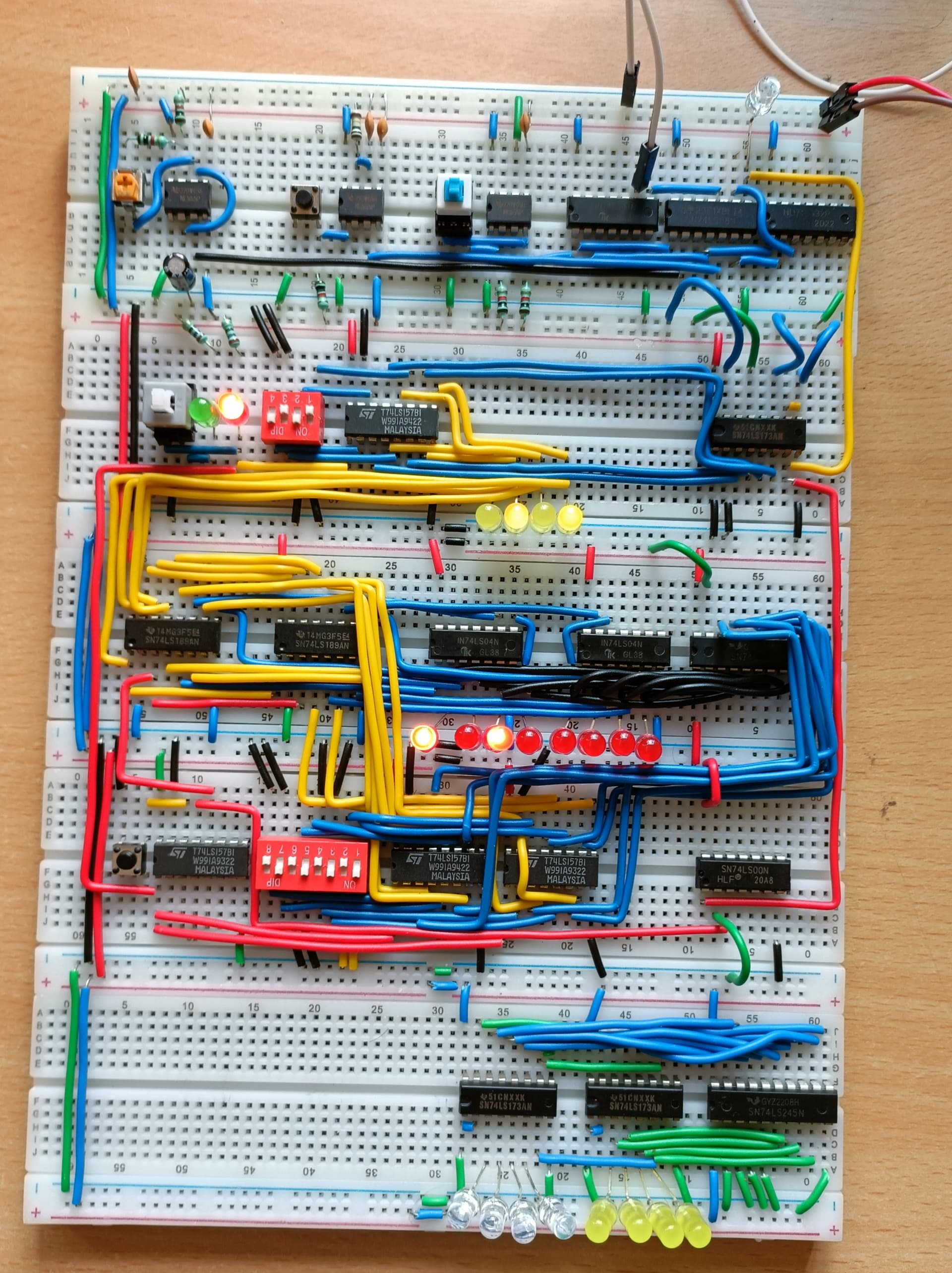
So I would like to describe the components that are present in the picture. At the tops of the picture there is a single breadboard that is the clock of the CPU and provides regular pulses to the CPU. Then there is a single breadboard on the left side of the picture consisting of only LEDs, this is working as a temporary bus for transferring data between the registers and the ALU of the CPU.
So now lets come to the three breadboard setup that is placed to the right of the picture. Here there are three parts the top and the bottom breadboard are the two registers that I have already build and explained earlier. Today I will be sharing the details about the components of the breadboard in the middle. This is the ALU of the CPU.
So this ALU contains some chips 74LS245(Octal Bus Transceiver), 74LS283(4 bit adder), 74LS283, and 74LS86(XOR gate), 74LS86; the chips are in order from left to right.
So 74LS245 as before is the chip responsible for maintaining communication between the bus and the ALU.
Then the 74LS283 chips are responsible for adding the values present in the register A and B. Here the 74LS283 chips are directly connected to the register A as shown in the picture. And are connected to the register B through the 74LS86, XOR gates.
The register B is connected to the adder through a XOR gate is to provide us with a way to subtract two number. That’s it!
To see the ALU in action please head over to this LinkedIn Profile .
Regards
Arghadeep Saha
Hi @Arghadeep_Saha,
Thanks for the update.
The project is getting complex, keep going, you’re on the right way.
OK… I “almost” understand your decision…
I’m really curious about your project.
If I’m not mistaken, I believe you’re using the Arduino Uno Rev3 as the power supply for your project, which outputs 5V at 1A max.
You’re already using 17 ICs and 36 LEDs. The Aurduino Uno may not be the most suitable power supply for your project.
In order not to interfere too much with your project, if I were building it, I would add decoupling capacitors because of the noise.
You’re distributing the power between breadboards by daisy chain connection. If I were doing the project, I’d distribute it by star connection.
Something on this subject:
Power distribution troubles across many breadboards
How do I connect multiple drivers or controllers to a single power supply?
I’ve re-read the thread, but I can’t find any information about the CPU. What are you using as the CPU?
Do you have any schematics or block diagrams you can share?
Sorry to give my opinion and ask so many questions.
I’d like you to keep us informed.
Good luck with the project
Jorge
I am not going to knock your project, think it’s a really great way to learn electronics and simple computing processes I stand in admiration on what you have done so far, think I would have given up quite a way back.
Only negative comment would come from a apple background as to just how many wires and layout the two Steve’s would have fit seeing this. Perhaps the next part is to look at the layout and see how it could be improved. But if you were going to draw the circuit board from this another great learning opportunity.
Please keep us posted on progress it’s really interesting
First of all ThankYou for helping me find out the problem in the power distribution. I will surely take take of that problem.
Yes I am using the Arduino to power the project but will soon be power this with the help of a 5V 2A DC power adapter. And will surely look into the power distribution.
Yes I almost forgot to add the decoupling capacitors, but am a little confused. See I used the power strips as a common power strip to power various part of the circuit. And various part of the circuit uses different values of capacitor. So I need to see how to connect them. If you have any suggestions for me please feel free to comment below.
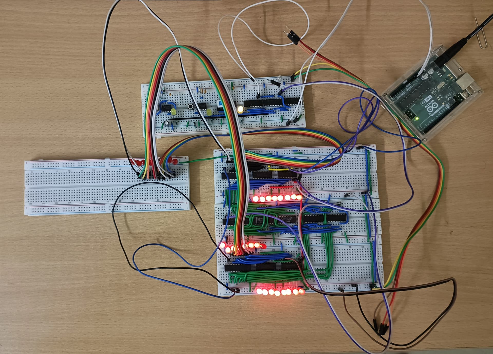
From a neutral stand point not very happy neither very sad I would like to share with you all about my recent updates of this project.
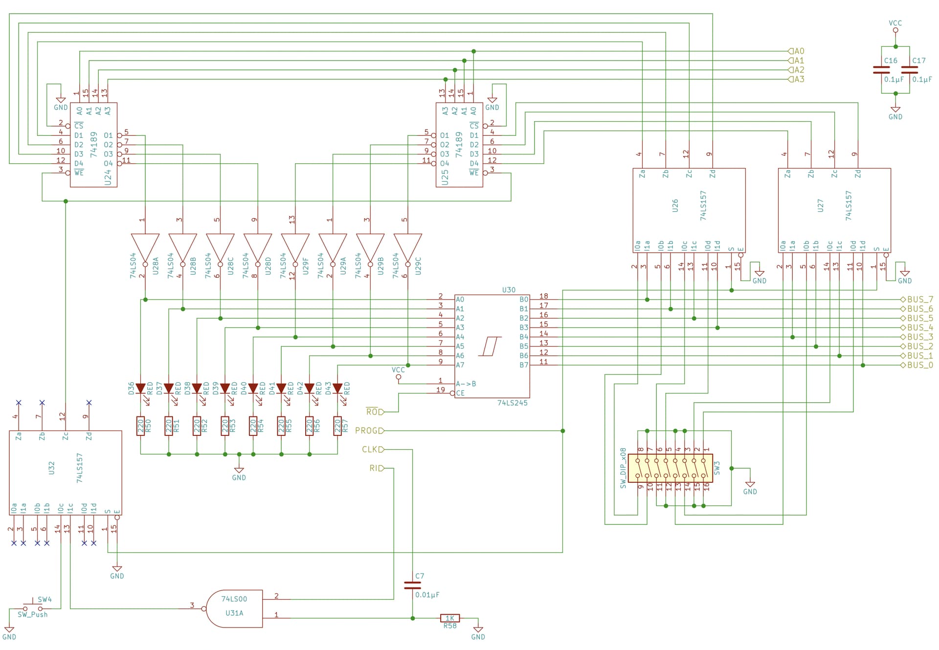
So I am working on the RAM module for the CPU for past few weeks. Although I built the module using 74LS189, 4-bit register as the primary storage for the RAM module. Then I also added two modes in the RAM module one is the PROGRAM mode and the other is the RUN mode.
In the RUN mode the program would run from the memory and in the PROGRAM mode I will be able to program the CPU with the help of two dip switches that I included in the circuit. The smaller dip switch with 4 switches serves the purpose of accessing various addresses on the two 74LS189 chips. And the larger dip switch with 8 switches help me to set the 8-bit data at that address. This is all about the memory module I will include the schematic diagram for this.
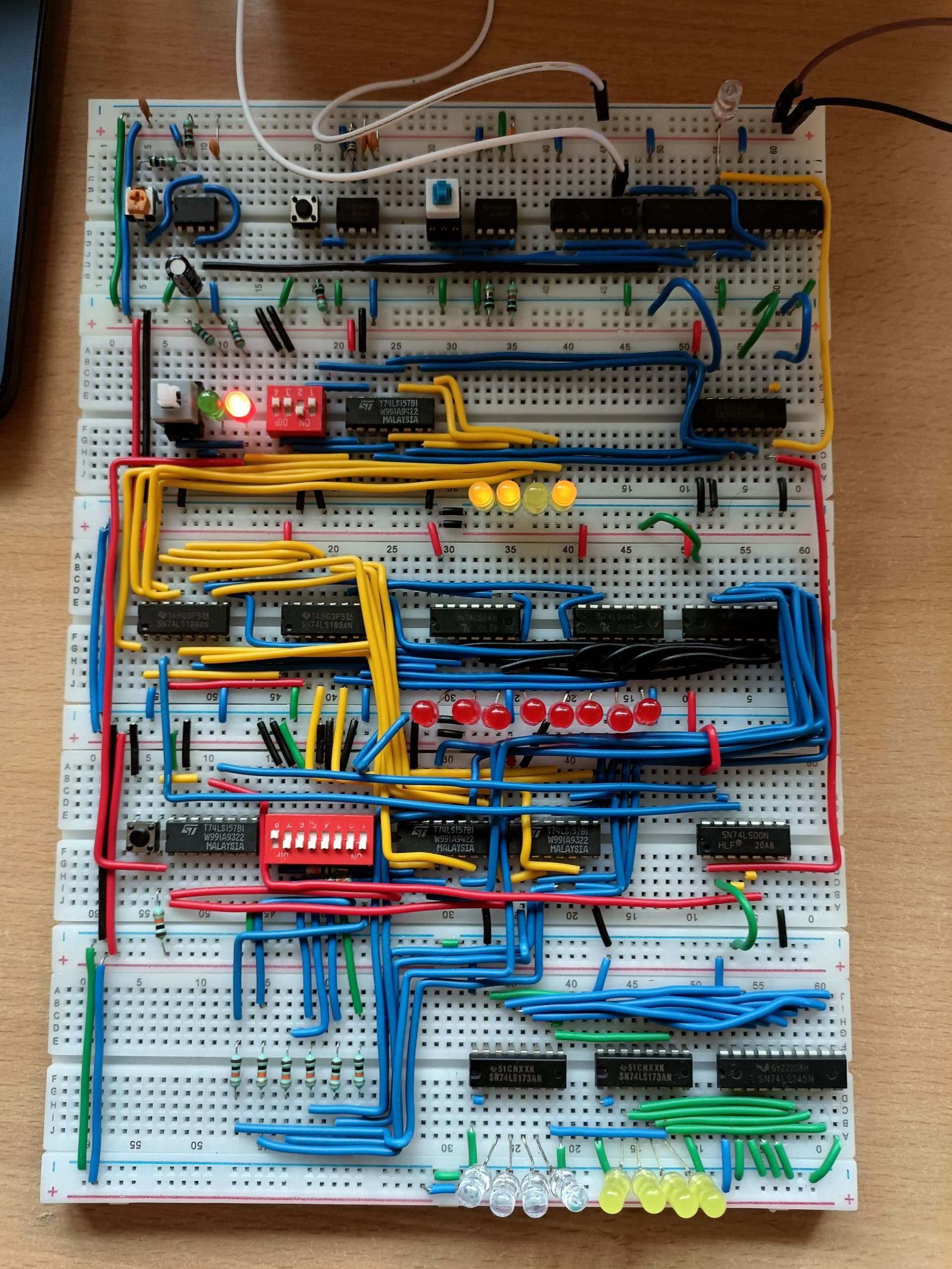
Now comes the sad part despite build it with utmost care the RAM module doesn’t work as intended. The values doesn’t stay constant in the 74LS189 chip and the values changes when I change modes from PROGRAM mode to RUN mode and vice versa. So after troubleshooting the circuit I am suspecting one problem that may have occurred in the circuit, this problem may be caused due to the problem in the signal integrity in the circuit, which is caused due to some construction constrains of the 74LS189 chip. So to address that I tried some ways like using NOT gates. But it still does not give me the expected result of latching on to the data that I give it.
Initial circuit:
After troubleshooting and modifying the circuit, yet it does not work as expected.
Schematic for Memory address register:
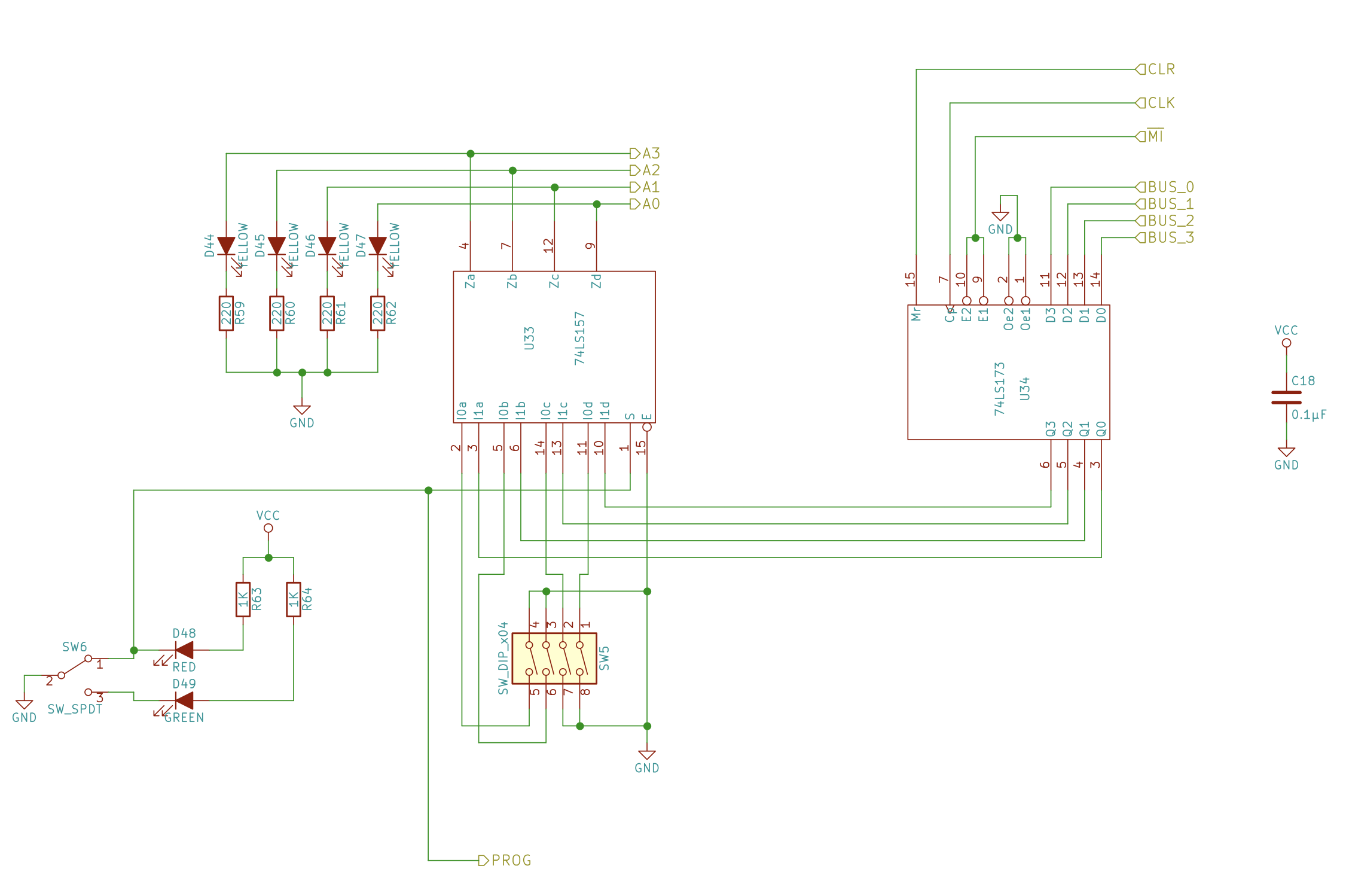
Schematic for the RAM Module:
Modified RAM Module:
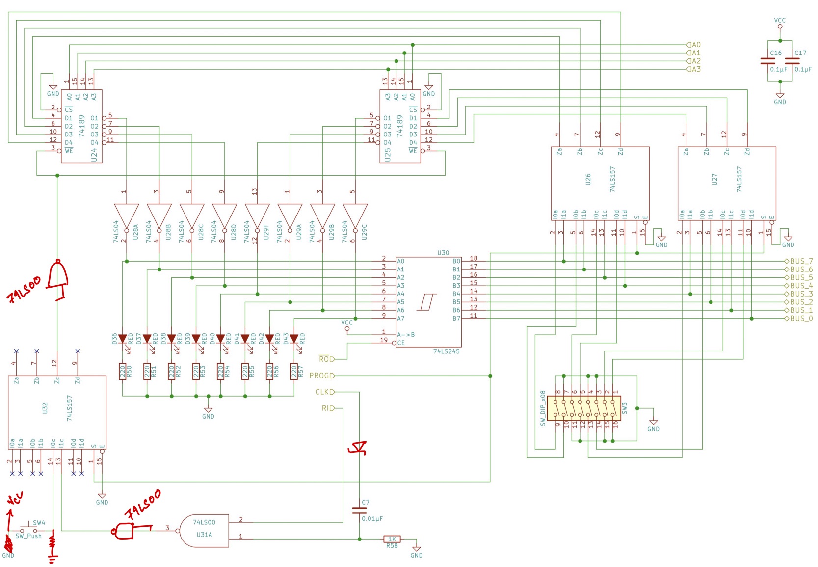
But the problem still persists. If anyone have any suggestion please feel free to comment below.
Arghadeep
Hi @Arghadeep_Saha,
I’m sorry, but I didn’t understand what you wanted to know. I think it’s my mistake for using the translator.
Can you explain what you want to know?
If you want, you can even draw a diagram/schematic by hand
Jorge
Hi @Arghadeep_Saha,
You should be happy!
congrats on what you’ve done so far.
I haven’t analyzed the circuit, I’ve just had a look at it, but I think you’re entering a critical phase of the project: problems with the power supply, noise caused by the breadboards, correcting errors both in the design and in the implementation of the circuit on the breadboards.
I had already mentioned the problems with the power supply, the the lack of decoupling capacitors and the lack of resistors in the LEDs.
I have a few questions for you if you don’t mind (sorry my schematic was hand-drawn).
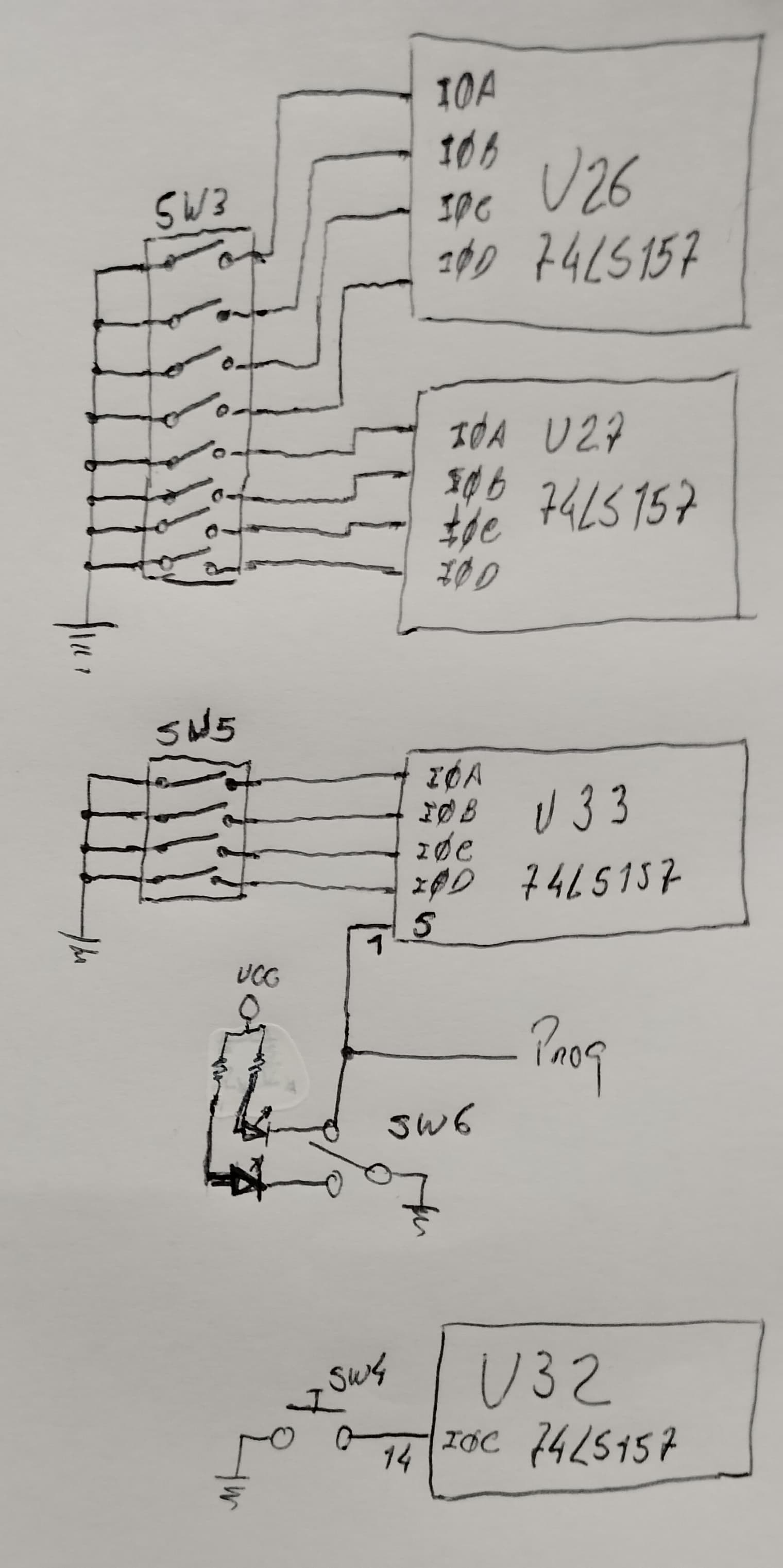
In ICs U26, U27 and U33, what are the values of I0a, I0b, I0c and I0d when the DIP switches SW3 and SW5 are not switched to ground?
In IC U33, what is the value of S (select) when SW6 is switched to ground?
In U32, what is the value of I0c when SW4 is not pressed?
If you have a multimeter, what is the voltage between pins 8 and 16 of the U24?
Be careful not to short-circuit the ICs if you do.
Jorge
I wanted to say that the power strips in the breadboard are all connected in parallel to the power sources. So if i add capacitors to reduce the noise in the circuit then since the power strips are connected in parallel so the capacitor values will add up and lead to a huge value of capacitance in the circuit which may lead to charge accumulation.
Sorry I will surely give you these values soon. I am currently unable to supply these values cause currently i am powering this circuit with an Arduino which supply a voltage of 3.5V and a current of 1A which is not the ideal operating condition. Once i get the adapter to supply voltage and current to the chips at an optimum level i will surely give you these values. Or is it ok if I supply you the values I currently have?
Hi @Arghadeep_Saha ,
thank you for your feedback.
I’m sorry that perhaps I wasn’t explicit with my questions, so I’m going to rephrase my questions using an example I made, but which in short is identical to your schematic.
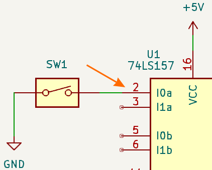
In this example I use the 75LS157 and just one DIP switch.
I’m asking, if you don’t mind (if you don’t know, let us know so we can help):
-
If the DIP switch has a closed contact, as it is grounded, the logic value on pin 2 of IC U1 is 0, correct?
-
And if the DIP switch is open, what is the logic value on pin 2 of IC U1?
In short, what is the logic value and voltage on pin 2 of IC U2 when SW1 is open?
| SW1 | Logic Value | Voltage |
|---|---|---|
| Close | 0 | 0V |
| Open | … | … |
These questions summarize the questions I asked in the previous post
Are you using 3.5V or 5V? Could you please confirm?
Yes, I’d like to know, even with the Arduino power supply.
What is the voltage between pins 8 and 16 of the U24?
Be careful not to short-circuit the ICs if you do.
The subject of decoupling capacitors is for a next post, OK?
I know this isn’t an electronics forum, but you’ve asked for help and we’ll do what we can.
Jorge
So the logic value of pin 2 when the dip switch is open is 1. The 74LS157 these are the TTL chips and has a resistor inside that ties the input to the Vcc and hence if we keep the dip switch open then by default the logical value in pin 2 is 1, that’s why I connect the other end of the dip switch to the ground and if you see my circuit on the breadboard and also in the schematic the dip switch is actually placed upside down.
I am powering the circuit currently using a 3.5 V source from Arduino.
Ok so I measured the voltage between the pin 8 and 16 of the U24 and the voltage was about 3.42V.
Thank you for sharing your thoughts on my project. It really helps me to dive deep in my project and acquire more knowledge, especially through these discussions.
Arghadeep
My friend @Arghadeep_Saha,
Thanks for your reply.
I’m the one who thanks you, because I’m really enjoying our conversation.
Now I need your help, if you don’t mind.
Could you please help me understand what you’ve written?
As you can see from my photo, I’m already an old man and my memory is very rusty and my knowledge of electronics isn’t very good…
-
What is a TTL chip and what does it means?
-
You say that " TTL chips and has a resistor inside that ties the input to the VCC and hence if we keep the dip switch open then by default the logical value in pin 2 is 1". Do you know where I can read more about this information?
-
Do you have the datasheet for your 74LS157? Could you please post the datasheet link here?
-
Do you have the equivalent schematic of the 74LS157 input port that you can post here so I can see what it looks like?
-
The voltage on the rails next to IC U24 is 3.42V. What is the minimum VCC value for this IC?
-
What does 74xx stand for?
-
And LS in 74xx?
Note: Just answer the questions you know or want to. I’ll try to find out the rest on the web, but I’d like to hear it from you.
I believe that, with mutual support, you’ll be able to take your project a step further.
Good luck with your project.
Stay motivated because it’s an excellent project
Jorge